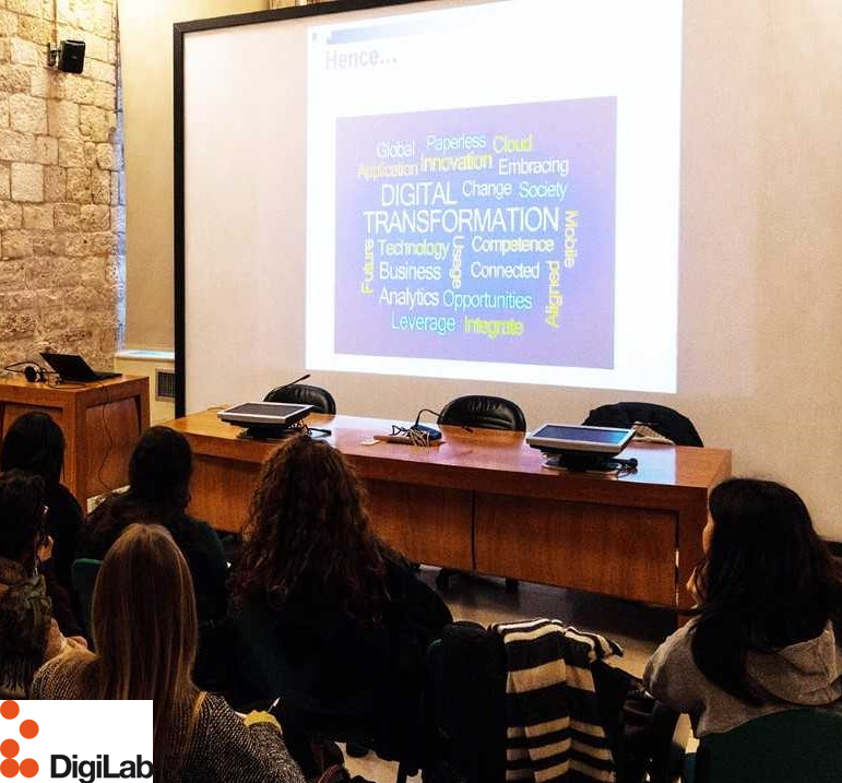
GENERATION OF NEW BUSINESS IDEAS
Design and characterization of plasmonic nanostructures for applications in sensors, photovoltaics, near field enhancement.
Design and characterization of nanoantennas for optical wireless network on.chip.
- Design and characterization of plasmonic nanostructures for applications in sensors, photovoltaics, near field enhancement.
- Design and characterization of nanoantennas for optical wireless network on.chip.
- Design and cha
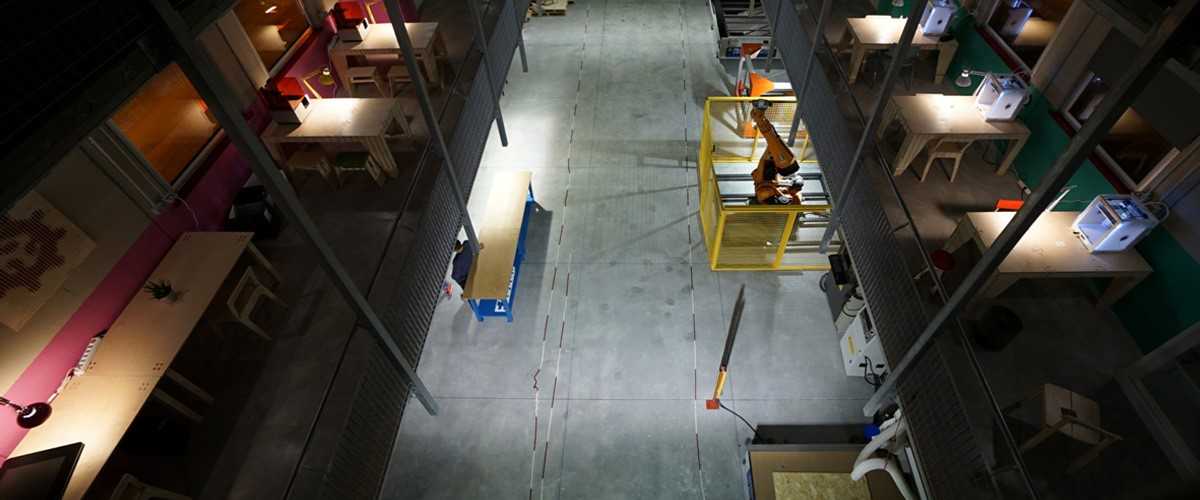
The Laboratory Fab Lab POLIBA is conformed with an interdisciplinary scientific structure for allowing the transversal collaboration of more "scientific knowledge" aimed especially at the experimental development of prototypes in the sectors of ar
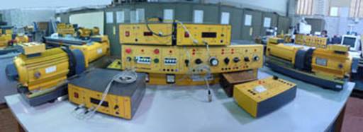
• ELECTRICAL DRIVES FOR ROBOTICS AND INDUSTRIAL AUTOMATION
- Evolutionary Algorithms for identification and control
- Control techniques for mobile robots and industrial manipulators
Intelligent systems based on artificial vision paradigms.
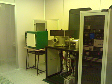
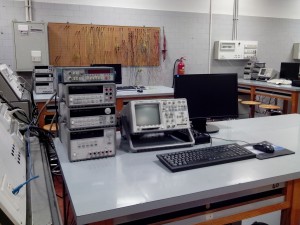
The Optoelectronics Laboratory exhibits expertise in the modeling, design, simulation, fabrication, and c
- Smart instruments for measurements on components and systems
- Model identification, parameters estimation and characterization of electrical machines, equipment, apparatus and electrical drives
- Development and characteriz
The scientific activity concerns the following 2 main topics of the Electrical Engineering:
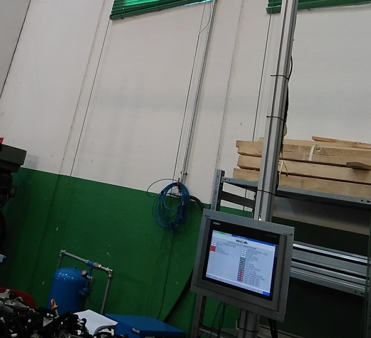
The Electrical and Electronic Measurement Lab activities are, among others, mainly focused on two institutional objectives: didactics for bachelor/master of science/doctoral degree and applied as well as theoretical research in the areas of: A/D c