AP Lab
Lab full name
Apulia regional laboratory of characterization of new organicand nanostructured materials
ERC 2nd Level Code
ERC 3rd level Code
Research Activities
- Design and characterization of plasmonic nanostructures for applications in sensors, photovoltaics, near field enhancement.
- Design and characterization of nanoantennas for optical wireless network on.chip.
- Design and characterization of beam steering from subwavelength apertures in metal substrates.
- Polymeric sensors for biomedical and industrial applications.
- Design and characterization of optical interconnecting devices for chip multiprocessor architectures.
- Design and characterization of III-V-N of semiconductor active photonic devices and photonic crystals for laser applications.
- Design, fabrication and characterization of integrated optical devices by sputtering, ion-exchange, spin-coating techniques.
Department
Contact Person
Companies and Institutions
National Nanotechnology Laboratory (NNL), CNR Istituto di Nanoscienze – Lecce (Italy)
Centro di nanotecnologie bio-molecolari, Istituto Italiano di Tecnologia (IIT) – Arnesano – Lecce (Italy)
Institute of Inorganic and Plasmas Methods, IMIP-CNR (Italy),
Microphotonics Group – St. Andrews University (UK)
Department of Materials Science, University of Patras (Greece)
LAAS-CNRSM, Toulose (France)
Projects
Progetto di ricerca " Ottimizzazione delle proprietà ottiche e di trasporto di strati di graphene da impiegare in celle ad eterogiunzione a-Si:H/c-S"
Progetto Galileo 2018 Italia-Francia "Selective nanotweezers based on integrated plasmonic resonators for environmental monitoring"
PRIN 2015 dal titolo "Wireless Networks through on-chip Optical Technology - WiNOT"
Progetto Galileo Italia-Francia 2014 "Experimental demonstration of mesoscopic self-collimation guiding"
Progetto Regionale "Laboratorio Regionale di Sintesi e caratterizzazione di nuovi materiali organici e nanostrutturati per Elettronica, Fotonica e Tecnologie Avanzate"
FIRB 2008 dal titolo "PHOTONICA - Photonic Interconnect Technology for Chip Multiprocessing Architectures"
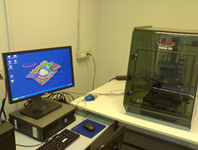
Facilities
• Spectrometric Ellipsometer,
• micro-controlled surface Profilometer,
• System for the deposition of thin films made of Spin coater,
• UV lamp and heating plate,
• Instrumentation for the characterization of thin films made of polarizing microscope including a BF/DF optical Kit.
Services
Characterization of thin films.
Measure of roughness and depth of optical films.
Deposition of polymeric film on glass substrates by spinning technique.
StakeHolder
Address / How to reach us
Via Re David 200, Bari, c/o Department of Electrical and Information Engineer
Hours
From Monday to Friday: hours 9:00-17:00
Area (mq)
20
Link to external content