
• Smart instruments for measurements on components and systems
• Development of measuring system for health monitoring and wearable sensors
• Analysis of biomedical signal
• Medical image processing

- Design and prototyping of PC-, microcontroller- and DSP-based mixed signals Data Acquisition (DAQ) and Data Processing Systems
- Industrial circuits, PLC programming and machines diagnostic for faults prevention
- Wireless S
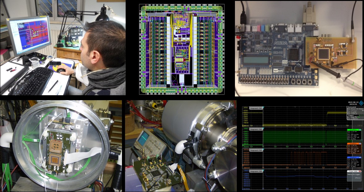
The lab has long been involved in the development and characterization of multichannel integrated circuits for read-out of solid-state detectors and sensors for high energy physics and medical imaging.
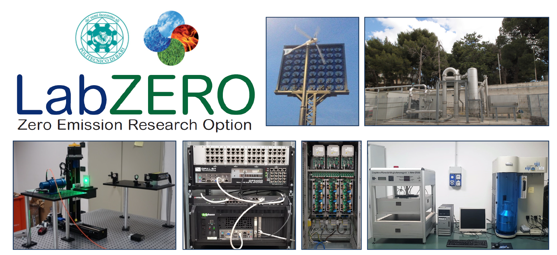
LabZERO is a multidisciplinary laboratory to enable strategic cooperation with enterprises and promote multidisciplinary research for the development of innovative technologies in the areas of ener
Design and characterization of plasmonic nanostructures for applications in sensors, photovoltaics, near field enhancement.
Design and characterization of nanoantennas for optical wireless network on.chip.
- Design and characterization of plasmonic nanostructures for applications in sensors, photovoltaics, near field enhancement.
- Design and characterization of nanoantennas for optical wireless network on.chip.
- Design and cha
- Smart instruments for measurements on components and systems
- Model identification, parameters estimation and characterization of electrical machines, equipment, apparatus and electrical drives
- Development and characteriz

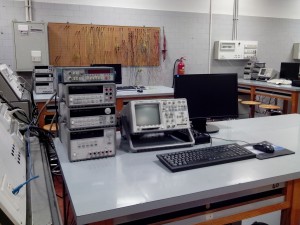
The Electrical and Electronic Measurement Lab activities are, among others, mainly focused on two institutional objectives: didactics for bachelor/master of science/doctoral degree and applied as well as theoretical research in the areas of: A/D c

The research activities of Electromagnetic Fields and Telecommunications Laboratory at Magna Grecia Center in Taranto and of Microwave and Optical Engineering (MOE) Laboratory in Bari are performed by the Microwave and Optical Engineering (MOE) gr
Development of Micro and Nano Devices models for Computer Aided Design and their Characterization