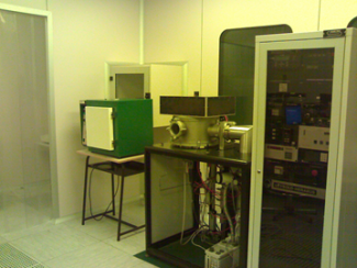
Clean Room
Lab full name
Clean Room
ERC 2nd Level Code
ERC 3rd level Code
Research Activities
Design and characterization of plasmonic nanostructures for applications in sensors, photovoltaics, near field enhancement.
Design and characterization of nanoantennas for optical wireless network on.chip.
Design and characterization of beam steering from subwavelength apertures in metal substrates.
Polymeric sensors for biomedical and industrial applications.
Design and characterization of optical interconnecting devices for chip multiprocessor architectures.
Design and characterization of III-V-N of semiconductor active photonic devices and photonic crystals for laser applications.
Design, fabrication and characterization of integrated optical devices by sputtering, ion-exchange, spin-coating techniques.
Department
Contact Person
Companies and Institutions
National Nanotechnology Laboratory (NNL), CNR Istituto di Nanoscienze – Lecce (Italy)
Centro di nanotecnologie bio-molecolari, Istituto Italiano di Tecnologia (IIT) – Arnesano – Lecce (Italy)
Institute of Inorganic and Plasmas Methods, IMIP-CNR (Italy)
Microphotonics Group – St. Andrews University (UK)
Department of Materials Science, University of Patras (Greece)
LAAS-CNRSM, Toulose (France)
Projects
Progetto di ricerca " Ottimizzazione delle proprietà ottiche e di trasporto di strati di graphene da impiegare in celle ad eterogiunzione a-Si:H/c-S"
Progetto Galileo 2018 Italia-Francia "Selective nanotweezers based on integrated plasmonic resonators for environmental monitoring"
PRIN 2015 dal titolo "Wireless Networks through on-chip Optical Technology - WiNOT"
Progetto Galileo Italia-Francia 2014 "Experimental demonstration of mesoscopic self-collimation guiding"
Progetto Regionale "Laboratorio Regionale di Sintesi e caratterizzazione di nuovi materiali organici e nanostrutturati per Elettronica, Fotonica e Tecnologie Avanzate"
FIRB 2008 dal titolo "PHOTONICA - Photonic Interconnect Technology for Chip Multiprocessing Architectures"
Facilities
Clean room in class 100-1000 equipped with chemical hood,
thermostat oven for ion exchange,
spin coater and DC - AC sputtering equipment.
Services
Fabrication and characterization of integrated optical devices by sputtering, ion-exchange, spin-coating techniques.
Deposition of dielectric or metal thin films on optical substrates with high degree of purity.
Treatments for the cleaning of optical subsatrates.
StakeHolder
Address / How to reach us
Via Re David 200, Bari, c/o Department of Electrical and Information Engineer
Hours
Hours (*) From Monday to Friday: hours 9:00-17:00
Area (mq)
20
Link to external content