AE&M Lab
Lab full name
Applied Electronics and Microelectronics
ERC 2nd Level Code
ERC 3rd level Code
Research Activities
The lab has long been involved in the development and characterization of multichannel integrated circuits for read-out of solid-state detectors and sensors for high energy physics and medical imaging. Another related activity is the characterization of detectors, sensors and electronic devices. In more detail, the main current research lines are the following:
Design of multichannel mixed-signal integrated circuits (ASIC) for the read-out of solid-state detectors used in high energy physics experiments and medical imaging applications
- Development of sensor interface electronics for environmental monitoring
- Prototyping (via access to the European consortium EUROPRACTICE) and characterization of integrated circuits
- Design and realization of hardware/firmware systems based on programmable devices (FPGA)
- Characterization of solid-state detectors for physics experiments and medical imaging applications (Silicon Photomultipliers)
Department
Contact Person
Technical Staff
Vincenzo Scarola, Gennaro Gelao
Companies and Institutions
SLAC Stanford, Menlo Park (CA, USA)
CERN, Geneva (Switzerland)
Munster Technological University, Cork (Ireland)
Istituto Nazionale di Fisica Nucleare
Fbk-IRST, Trento
AVIO AERO, Bari
ETG Risorse, Chivasso (To)
ITEL, Ruvo di Puglia
Matrix s.r.l., Conversano (Ba)
Cupersafety s.r.l., Conversano (Ba)
Microlaben s.r.l.(spin-off company of Politecnico di Bari)
Projects
CMS experiment (CERN – Geneva)
H2020 “PASSEPARTOUT” (European Community)
H2020 "EVOQUE" (European Community)
POC "SPHERE" PNRR
Research contract “Collaboration on the development of a Time-of-Flight (ToF) readout system for Silicon Photon Multipliers” (SLAC Stanford)
Innolabs “Sistema partecipativo attivo per la sensibilizzazione delle comunità al rischio di esposizione al GAS RADON” (Apulia Regional government)
PON “FURTHER - FUture Rivoluzionarie Tecnologie per velivoli più Elettrici” (MIUR)
Funding
MIUR – 445 k€
SLAC Stanford – 34 k€
Apulia Regional government – 20 k€
European Community – 120 k€
Politecnico di Bari – 6 k€
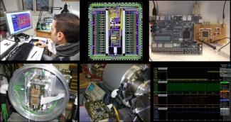
Facilities
-Linux workstations for IC design, equipped with the suite Cadence IC
-Semi-automatic probestation Karl Suss PM8, optical microscope 50X Karl Suss
-Logic state analyzer Tektronix, 32 channels
-Semiconductor parameter analyzers HP4145B and 4155B
-Spectrum analyzer Agilent N1996A, 100kHz-6GHz
-Oscilloscope DPO Tektronix 4GHz, 4 channels
-Oscilloscope Rohde-Schwarz 4GHz, 4 channels
-Arbitrary signal generator Tektronix, 200MHz
-Standard lab instrumentation (stabilized power supplies, digital multimeters, low-end oscilloscopes and function generators)
Softwares
Suite Cadence IC for electronic design
Services
IC design and prototyping, via EUROPRACTICE service (only for research and educational purposes, no commercial activities)
StakeHolder
Address / How to reach us
Via Orabona 4, 70125 – Bari (Italy)
Dipartimento di Ingegneria Elettrica e dell’Informazione
Plesso Salvatore, IV floor
DEI main building, II floor
Hours
Mon - Fri 9:00 - 17:30
Area (mq)
50